The Precision Grinding Role of Brown Fused Alumina Micropowder in the Semiconductor Industry
Friends, today we’re going to talk about something both hardcore and down-to-earth—brown fused alumina micropowder. You might not have heard of it, but the most crucial and delicate chips in your phone and smartwatch, before they were even manufactured, had likely dealt with it. Calling it the chip’s “chief beautician” is no exaggeration.
Don’t imagine it as a rough tool like a whetstone. In the world of semiconductors, it plays a role as delicate as a micro-sculptor using nanoscale scalpels.
I. The Chip’s “Face-Sculpting”: Why Grinding is Necessary?
Let’s first understand one thing: chips don’t grow directly on flat ground. They are “built” layer by layer on an extremely pure, flat silicon wafer (what we call a “wafer”), like constructing a building. This “building” has dozens of floors, and the circuitry on each floor is thinner than one-thousandth the thickness of a human hair.
So here’s the problem: when you’re building a new floor, if the foundation—the surface of the previous floor—is even slightly uneven, even with a protrusion as small as an atom, it can cause the entire building to be crooked, short-circuit, and render chips unusable. The losses are no joke.
Therefore, after each floor is completed, we must conduct a thorough “cleaning” and “leveling.” This process has a fancy name: “Chemical Mechanical Planarization,” abbreviated as CMP. While the name sounds complicated, the principle is not difficult to understand: it’s a combination of chemical corrosion and mechanical abrasion.
The chemical “punch” uses a special polishing fluid to soften and corrode the material to be removed, making it more “soft.”
The mechanical “punch” comes into play—brown corundum micropowder. Its task is to use physical methods to precisely and evenly “scrape” away the material that has been “softened” by the chemical process.
You might ask, with so many abrasives available, why this one in particular? That’s where its exceptional qualities come in.
 II. “Micronized Powder That’s Not So Micronized”: The Unique Skill of Brown Fused Alumina
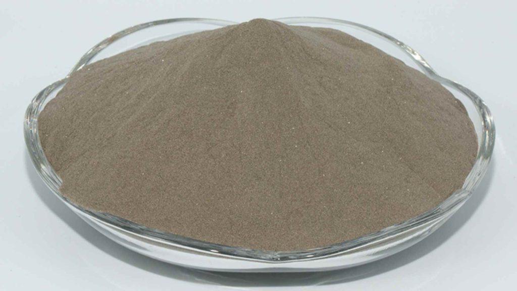
In the semiconductor industry, the brown fused alumina micronized powder used is no ordinary product. It’s a “special forces” unit, meticulously selected and refined.
First, it’s hard enough, but not reckless. Brown fused alumina‘s hardness is second only to diamond, more than enough to handle commonly used chip materials like silicon, silicon dioxide, and tungsten. But the key is that its hardness is a “tough” hardness. Unlike some harder materials (like diamond) that are brittle and easily break under pressure, brown fused alumina maintains its integrity while ensuring cutting force, avoiding becoming a “destructive element.”
Second, its narrow particle size ensures even cutting. This is the most crucial point. Imagine trying to polish a precious jade with a pile of stones of varying sizes. The larger stones would inevitably leave deep pits, while the smaller ones might be too small to work on. In CMP (Chemical Mechanical Polishing) processes, this is absolutely unacceptable. The brown fused alumina micropowder used in semiconductors must have an extremely narrow particle size distribution. This means that almost all particles are roughly the same size. This ensures that thousands of micropowder particles move in unison on the wafer surface, applying even pressure to create a flawless surface, not a pockmarked one. This precision is at the nanometer level.
Third, it’s a chemically “honest” agent. Chip manufacturing uses a wide variety of chemicals, including acidic and alkaline environments. Brown fused alumina micropowder is chemically very stable and doesn’t easily react with other components in the polishing fluid, preventing the introduction of new impurities. It’s like a hardworking, unassuming employee—the kind of person bosses (engineers) love.
Fourth, its morphology is controllable, producing “smooth” particles. Advanced brown fused alumina micropowder can even control the “shape” (or “morphology”) of the particles. Through a special process, particles with sharp edges can be transformed into near-spherical or polyhedral shapes. These “smooth” particles effectively reduce the “grooving” effect on the wafer surface during cutting, significantly lowering the risk of scratches.
III. Real-world Application: The “Silent Race” on the CMP Production Line
On the CMP production line, wafers are firmly held in place by vacuum chucks, surface down, pressed onto a rotating polishing pad. Polishing fluid containing brown fused alumina micropowder is continuously sprayed, like a fine mist, between the polishing pad and the wafer.
At this point, a “precision race” in the microscopic world begins. Billions of brown fused alumina micropowder particles, under pressure and rotation, perform millions of nanometer-level cuts per second on the wafer surface. They must move in unison, like a disciplined army, advancing smoothly, “flattening” the high areas and “leaving blank” the low areas.
The entire process must be as gentle as a spring breeze, not a raging storm. Excessive force can scratch or create microcracks (called “subsurface damage”); insufficient force leads to low efficiency and disrupts production schedules. Therefore, precise control over the concentration, particle size, and morphology of brown fused alumina micropowder directly determines the final chip yield and performance.
From the initial rough polishing of silicon wafers, to the planarization of each insulating layer (silicon dioxide), and finally to the polishing of the tungsten plugs and copper wires used for connecting circuits, brown fused alumina micropowder is indispensable in almost every critical planarization step. It permeates the entire chip manufacturing process, truly a “behind-the-scenes hero.”
IV. Challenges and the Future: There is no best, only better
Of course, this path has no end. As chip manufacturing processes advance from 7nm and 5nm to 3nm and even smaller sizes, the requirements for CMP processes have reached an “extreme” level. This presents even greater challenges for brown fused alumina micropowder:
Fineer and more uniform: Future micropowders may need to reach the tens of nanometer scale, with a particle size distribution as uniform as if sieved by a laser.
Cleaner: Any metal ion impurities are fatal, leading to increasingly higher purity requirements.
Functionalization: Will “intelligent micropowders” emerge in the future? For example, with specially modified surfaces, they could alter cutting characteristics under specific conditions, or achieve self-sharpening, self-lubricating, or other functions?
Therefore, despite its origins in the traditional abrasive industry, brown fused alumina micropowder has undergone a magnificent transformation once it enters the cutting-edge field of semiconductors. It is no longer a “hammer,” but a “nanosurgical scalpel.” The perfectly smooth surface of the core chip in every advanced electronic device we use owes its existence to the countless tiny particles.
This is a grand project conducted in the microscopic world, and brown fused alumina micropowder is undoubtedly a silent yet indispensable super craftsman in this project.
II. “Micronized Powder That’s Not So Micronized”: The Unique Skill of Brown Fused Alumina
In the semiconductor industry, the brown fused alumina micronized powder used is no ordinary product. It’s a “special forces” unit, meticulously selected and refined.
First, it’s hard enough, but not reckless. Brown fused alumina‘s hardness is second only to diamond, more than enough to handle commonly used chip materials like silicon, silicon dioxide, and tungsten. But the key is that its hardness is a “tough” hardness. Unlike some harder materials (like diamond) that are brittle and easily break under pressure, brown fused alumina maintains its integrity while ensuring cutting force, avoiding becoming a “destructive element.”
Second, its narrow particle size ensures even cutting. This is the most crucial point. Imagine trying to polish a precious jade with a pile of stones of varying sizes. The larger stones would inevitably leave deep pits, while the smaller ones might be too small to work on. In CMP (Chemical Mechanical Polishing) processes, this is absolutely unacceptable. The brown fused alumina micropowder used in semiconductors must have an extremely narrow particle size distribution. This means that almost all particles are roughly the same size. This ensures that thousands of micropowder particles move in unison on the wafer surface, applying even pressure to create a flawless surface, not a pockmarked one. This precision is at the nanometer level.
Third, it’s a chemically “honest” agent. Chip manufacturing uses a wide variety of chemicals, including acidic and alkaline environments. Brown fused alumina micropowder is chemically very stable and doesn’t easily react with other components in the polishing fluid, preventing the introduction of new impurities. It’s like a hardworking, unassuming employee—the kind of person bosses (engineers) love.
Fourth, its morphology is controllable, producing “smooth” particles. Advanced brown fused alumina micropowder can even control the “shape” (or “morphology”) of the particles. Through a special process, particles with sharp edges can be transformed into near-spherical or polyhedral shapes. These “smooth” particles effectively reduce the “grooving” effect on the wafer surface during cutting, significantly lowering the risk of scratches.
III. Real-world Application: The “Silent Race” on the CMP Production Line
On the CMP production line, wafers are firmly held in place by vacuum chucks, surface down, pressed onto a rotating polishing pad. Polishing fluid containing brown fused alumina micropowder is continuously sprayed, like a fine mist, between the polishing pad and the wafer.
At this point, a “precision race” in the microscopic world begins. Billions of brown fused alumina micropowder particles, under pressure and rotation, perform millions of nanometer-level cuts per second on the wafer surface. They must move in unison, like a disciplined army, advancing smoothly, “flattening” the high areas and “leaving blank” the low areas.
The entire process must be as gentle as a spring breeze, not a raging storm. Excessive force can scratch or create microcracks (called “subsurface damage”); insufficient force leads to low efficiency and disrupts production schedules. Therefore, precise control over the concentration, particle size, and morphology of brown fused alumina micropowder directly determines the final chip yield and performance.
From the initial rough polishing of silicon wafers, to the planarization of each insulating layer (silicon dioxide), and finally to the polishing of the tungsten plugs and copper wires used for connecting circuits, brown fused alumina micropowder is indispensable in almost every critical planarization step. It permeates the entire chip manufacturing process, truly a “behind-the-scenes hero.”
IV. Challenges and the Future: There is no best, only better
Of course, this path has no end. As chip manufacturing processes advance from 7nm and 5nm to 3nm and even smaller sizes, the requirements for CMP processes have reached an “extreme” level. This presents even greater challenges for brown fused alumina micropowder:
Fineer and more uniform: Future micropowders may need to reach the tens of nanometer scale, with a particle size distribution as uniform as if sieved by a laser.
Cleaner: Any metal ion impurities are fatal, leading to increasingly higher purity requirements.
Functionalization: Will “intelligent micropowders” emerge in the future? For example, with specially modified surfaces, they could alter cutting characteristics under specific conditions, or achieve self-sharpening, self-lubricating, or other functions?
Therefore, despite its origins in the traditional abrasive industry, brown fused alumina micropowder has undergone a magnificent transformation once it enters the cutting-edge field of semiconductors. It is no longer a “hammer,” but a “nanosurgical scalpel.” The perfectly smooth surface of the core chip in every advanced electronic device we use owes its existence to the countless tiny particles.
This is a grand project conducted in the microscopic world, and brown fused alumina micropowder is undoubtedly a silent yet indispensable super craftsman in this project. English
 Русский
 日本語
日本語 한국어
한국어 Español
 Tiếng Việt
 Deutsch
 Français
 Italiano
 Português