The Role of White Fused Alumina in Polishing Electronic Components
In this era of ubiquitous smartphones, computers, and various smart devices, the performance requirements for electronic components are constantly increasing. They need to be fast, small, and incredibly powerful. You might not know that achieving these requires a seemingly insignificant yet crucial step—polishing. And in this field, there is a quietly accomplished “hardcore craftsman”—white fused alumina.
Today, let’s unveil the mystery of this “craftsman” and discuss how it plays a vital role in the precision world of electronic components.
I. Getting to Know the Main Character: What exactly is White Fused Alumina?
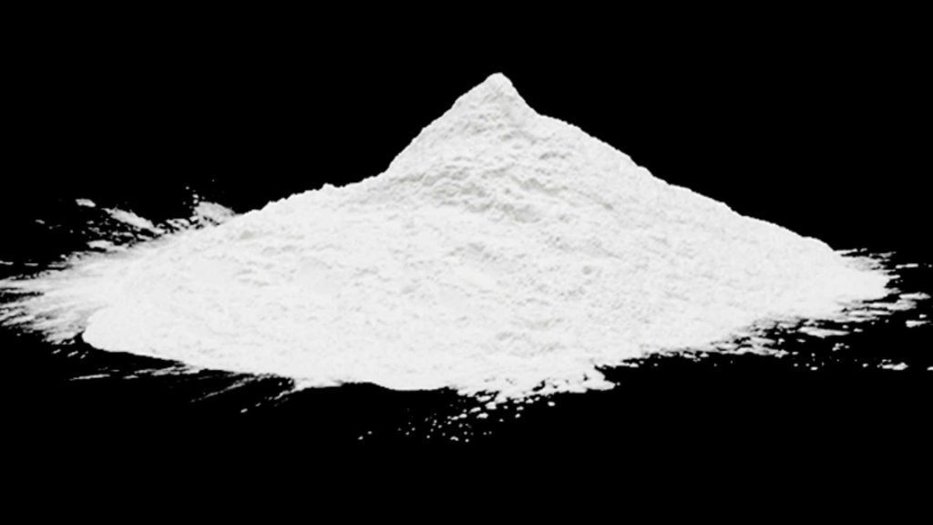
Simply put, white fused alumina is a highly pure synthetic corundum. Its main component is α-alumina (Al₂O₃). You can compare it to its siblings: for example, brown fused alumina contains slightly more impurities, hence its brownish color; while white fused alumina, because of its purer raw materials, produces white crystals after firing, with a “cleaner” texture.
How is it made? Simply put, it’s a process of “rebirth through fire.” High-quality alumina powder is melted, cooled, and recrystallized in a high-temperature electric arc furnace exceeding 2000 degrees Celsius. Finally, it is crushed and sieved to obtain white fused alumina abrasives of different particle sizes.
Don’t underestimate this process; it endows white fused alumina with several key properties, making it the ideal choice for polishing electronic components:
High hardness, truly “rigid”: Its Mohs hardness is as high as 9.0, second only to diamond and silicon carbide. This means that cutting and grinding other materials is a piece of cake, and it’s not easily worn down itself.
Moderate toughness, a balance of hardness and flexibility: Being only hard isn’t enough; too brittle, like glass shards, it breaks at the slightest touch and is unusable. White fused alumina possesses both high hardness and good toughness. Under pressure, it can break to a moderate degree, revealing new sharp edges, rather than turning into powder—this is called “self-sharpening.” This is like a self-healing miniature carving knife, constantly maintaining its sharpness.
Its excellent chemical stability makes it very “calm”: Various acidic and alkaline polishing solutions are frequently used in the polishing process. White fused alumina is chemically very stable and does not easily react with these chemical media, ensuring that the polishing process does not introduce accidental chemical contamination. This is extremely important in the electronics industry, where purity is paramount.
 II. How does white fused alumina “show off” in electronic component polishing?
Polishing electronic components is not as simple as just wiping something shiny. It is a “sculpting art” performed in the microscopic world, aiming to achieve a perfectly flat, absolutely smooth, and damage-free surface at the nanometer or even atomic level. White fused alumina is the main force in achieving this art.
1. The “foundation leveling” work for silicon wafers
Chips are manufactured on silicon wafers. You can imagine that if the foundation for a building is uneven, the building cannot be built, and electrical wires will be haphazardly strung. The same principle applies to chip manufacturing. Layers are stacked one on top of another. If any layer is uneven, subsequent photolithography will lose focus, leading to short circuits or open circuits.
This is where CMP (Chemical Mechanical Polishing) technology comes in, and white fused alumina microparticles often play a crucial role in the “mechanical work.” In the polishing slurry, countless tiny white fused alumina particles, like millions of tiny craftsmen, perform extremely small and uniform cuts on the silicon wafer surface under pressure and rotation. They gradually grind away the surface “peaks,” while relatively preserving the valleys, ultimately achieving overall extreme flatness. The hardness and self-sharpening properties of white fused alumina ensure that this process is efficient and consistent.
2. Surface Finishing of Semiconductor Devices
Inside a chip, in addition to silicon, there are metals (such as copper and tungsten) used for conductive lines and insulating layers (such as silicon dioxide) for isolation. These different materials have different hardness and removal rates. During polishing, excess metal needs to be removed without damaging the underlying insulating layer; this is called “high selectivity.”
White fused alumina micropowder plays a highly precise role here. By adjusting the chemical composition of the polishing slurry (the “chemical” part) and working synergistically with white fused alumina (the “mechanical” part), it’s possible to achieve highly efficient removal of certain materials (such as copper) while barely touching other materials (such as silicon dioxide). This pinpoint precision is crucial for ensuring chip yield.
3. The “Aesthetics Star” of Other Electronic Components
Besides high-precision chips, many electronic components we encounter daily also rely on white fused alumina polishing.
LED Sapphire Substrates: Many high-brightness LEDs use sapphire as their substrate. Sapphire itself has extremely high hardness, requiring white fused alumina—a “hard-on-hard” material—for polishing to achieve a mirror-like smooth surface, maximizing light extraction efficiency and making the LED brighter.
Quartz Crystal Resonators: These are the “heartbeat” components that provide clock signals to circuits. Their frequency stability requirements are extremely high, and their surface quality and thickness must be precisely controlled; white fused alumina polishing is perfectly suited for this task. Magnetic materials, glass substrates, and other materials also require white fused alumina during processing to achieve a final smooth and glossy finish.
III. Why White Fused Alumina? – A Summary of its Unique Advantages
Looking back, among many abrasives, why does the electronics industry favor white fused alumina?
Controllable Precision: Its particles can be made extremely fine and uniform (down to the micrometer level) with regular shapes. This ensures predictable and uniform polishing results, preventing surface scratches caused by inconsistent particle sizes.
Extremely Low Contamination: High purity means it generates very little metallic impurities during polishing, meeting the stringent cleanliness requirements of the semiconductor industry.
Balance of Efficiency and Quality: It is not as “hard” and expensive as diamond, nor as inefficient as soft abrasives. It achieves a perfect balance between hardness, toughness, and cost, making it a highly cost-effective choice.
So, the next time you pick up your phone and experience its smooth operation and powerful functions, imagine this: inside those tiny chips and delicate components, a silent and precise “surface revolution” involving countless white fused alumina microparticles has taken place. It is this unassuming “hardcore craftsman,” with its hardness and purity, that cleared the final nanometer-level barrier for the unimpeded flow of the electronic world. It may never stand in the spotlight, but it is an indispensable hero behind the scenes. Technological progress often lies hidden in these minute details, shining with the most simple yet captivating brilliance of materials science.
II. How does white fused alumina “show off” in electronic component polishing?
Polishing electronic components is not as simple as just wiping something shiny. It is a “sculpting art” performed in the microscopic world, aiming to achieve a perfectly flat, absolutely smooth, and damage-free surface at the nanometer or even atomic level. White fused alumina is the main force in achieving this art.
1. The “foundation leveling” work for silicon wafers
Chips are manufactured on silicon wafers. You can imagine that if the foundation for a building is uneven, the building cannot be built, and electrical wires will be haphazardly strung. The same principle applies to chip manufacturing. Layers are stacked one on top of another. If any layer is uneven, subsequent photolithography will lose focus, leading to short circuits or open circuits.
This is where CMP (Chemical Mechanical Polishing) technology comes in, and white fused alumina microparticles often play a crucial role in the “mechanical work.” In the polishing slurry, countless tiny white fused alumina particles, like millions of tiny craftsmen, perform extremely small and uniform cuts on the silicon wafer surface under pressure and rotation. They gradually grind away the surface “peaks,” while relatively preserving the valleys, ultimately achieving overall extreme flatness. The hardness and self-sharpening properties of white fused alumina ensure that this process is efficient and consistent.
2. Surface Finishing of Semiconductor Devices
Inside a chip, in addition to silicon, there are metals (such as copper and tungsten) used for conductive lines and insulating layers (such as silicon dioxide) for isolation. These different materials have different hardness and removal rates. During polishing, excess metal needs to be removed without damaging the underlying insulating layer; this is called “high selectivity.”
White fused alumina micropowder plays a highly precise role here. By adjusting the chemical composition of the polishing slurry (the “chemical” part) and working synergistically with white fused alumina (the “mechanical” part), it’s possible to achieve highly efficient removal of certain materials (such as copper) while barely touching other materials (such as silicon dioxide). This pinpoint precision is crucial for ensuring chip yield.
3. The “Aesthetics Star” of Other Electronic Components
Besides high-precision chips, many electronic components we encounter daily also rely on white fused alumina polishing.
LED Sapphire Substrates: Many high-brightness LEDs use sapphire as their substrate. Sapphire itself has extremely high hardness, requiring white fused alumina—a “hard-on-hard” material—for polishing to achieve a mirror-like smooth surface, maximizing light extraction efficiency and making the LED brighter.
Quartz Crystal Resonators: These are the “heartbeat” components that provide clock signals to circuits. Their frequency stability requirements are extremely high, and their surface quality and thickness must be precisely controlled; white fused alumina polishing is perfectly suited for this task. Magnetic materials, glass substrates, and other materials also require white fused alumina during processing to achieve a final smooth and glossy finish.
III. Why White Fused Alumina? – A Summary of its Unique Advantages
Looking back, among many abrasives, why does the electronics industry favor white fused alumina?
Controllable Precision: Its particles can be made extremely fine and uniform (down to the micrometer level) with regular shapes. This ensures predictable and uniform polishing results, preventing surface scratches caused by inconsistent particle sizes.
Extremely Low Contamination: High purity means it generates very little metallic impurities during polishing, meeting the stringent cleanliness requirements of the semiconductor industry.
Balance of Efficiency and Quality: It is not as “hard” and expensive as diamond, nor as inefficient as soft abrasives. It achieves a perfect balance between hardness, toughness, and cost, making it a highly cost-effective choice.
So, the next time you pick up your phone and experience its smooth operation and powerful functions, imagine this: inside those tiny chips and delicate components, a silent and precise “surface revolution” involving countless white fused alumina microparticles has taken place. It is this unassuming “hardcore craftsman,” with its hardness and purity, that cleared the final nanometer-level barrier for the unimpeded flow of the electronic world. It may never stand in the spotlight, but it is an indispensable hero behind the scenes. Technological progress often lies hidden in these minute details, shining with the most simple yet captivating brilliance of materials science. English
 Русский
 日本語
日本語 한국어
한국어 Español
 Tiếng Việt
 Deutsch
 Français
 Italiano
 Português